News & Events
24th April 2024
We held the final meeting of the PowerElec project in Vienna in April 2024 hosted by TU Wien. With just one month left of the project it was great to share the technical results and review the huge amount of progress we have made together over the last 3 years.

30th August 2023
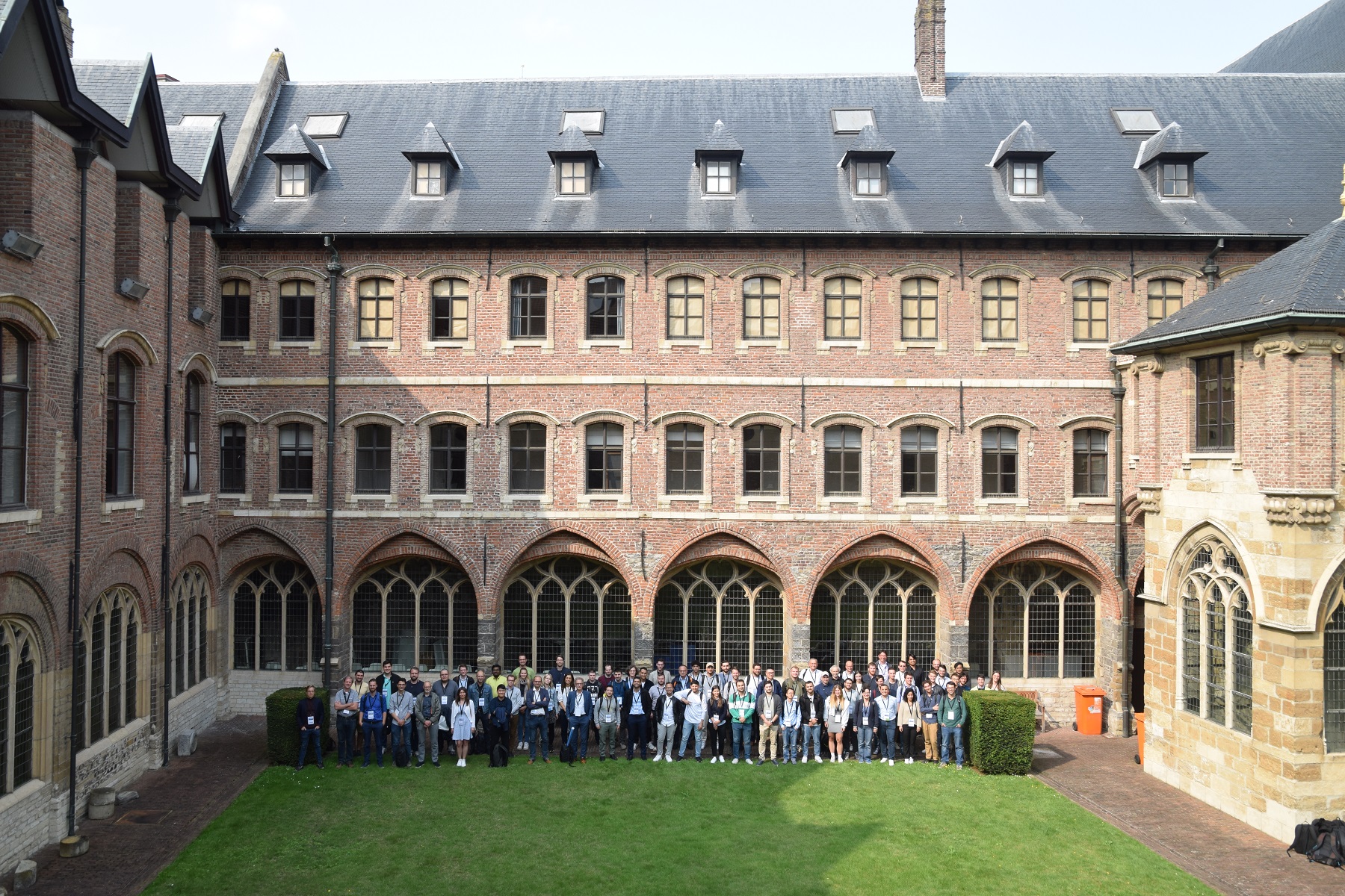
YESvGaN-TRANSFORM-PowerElec PhD summer school - GaN and SiC power electronics: From basics to application
The YESvGaN-TRANSFORM-PowerElec PhD summer school, 28th-30th August 2023 was a great success! Interesting and inspiring talks, enthusiastic participants and an amazing atmosphere were lasting until late in the evening. Thank you to everyone that was involved to make this event possible, educational and enjoyable.
A greener future requires minimizing the waste of energy. Electric power needs to be converted (multiple times) during its way from primary energy supply to the electronic devices used in our daily lives e.g. from the 220V AC mains to a 12V DC end-user appliance. Key to reducing the energy consumption is thus to maximize the efficiency in power conversion. This efficiency can be drastically improved by replacing power transistors that are currently based on silicon by wide band gap (WBG) semiconductors such as gallium nitride (GaN) and silicon carbide (SiC). Despite an accelerating adoption of GaN and SiC during the last years for consumer power supplies and automotive inverters, respectively, silicon-based technology is still largely dominating. To unlock the full potential of WBG based devices, we need to study and understand all the different aspects of the power devices, from growing the raw material to packaging and a demonstration of its potential in a final device.
This PhD summer school focused on the production and development of GaN and SiC wide band gap power transistor devices. The attendees got a full overview, from growing the raw wide-bandgap materials until packaging for the final application:
- How wide band gap semiconductors differ from conventional Si semiconductor technology and the physical properties of each material.
- How to implement the semiconductor material in the device via epitaxial film growth and how to characterize the materials to correlate the processing details to the final properties of the device.
- How reliable the performance of the final devices is and how to control and improve the reliability.
- How to produce the power devices on large scale and what the future will bring.
Each aspect was thoroughly discussed during a lecture given by invited experts from academia and industry which are working at the forefront of this field. The summer school is recognized as a specialist course from the Doctoral Schools of Ghent University. After successful participation, the Doctoral Schools will add this course to your curriculum. Keep in mind that this takes up to one to two months after completion of the course.
This summer school was co-organized by the ESCEL JU funded YESvGaN project (grant no 101007229), KDT JU funded TRANSFORM project (grant no 101007237) and the EMPIR funded PowerElec project (grant no 20IND09). The summer school was supported by the Flemish Government and the doctoral schools of Ghent University.
16th January 2023
Session on SPIE Optical Metrology conference
A special session on the application of compressed sensing to metrology is organised by consortium members within the SPIE Optical Metrology conference (Modeling Aspects in Optical Metrology IX) in Munich 26-29 June 2023. Click here for more details.
16th January 2023
PowerElec project session at SMSI conference
A special session for the PowerElec project is organised at the Sensor and Measurement Science International (SMSI) Conference, Nuremberg, May 8-11, 2023. Click here for more details.
23rd September 2022
First PowerElec deliverable successfully finalised
The first deliverable of the PowerElec project was successfully submitted in August and accepted in September by EURAMET. This first deliverable was titled “Report on capabilities and limitations of advanced sampling strategies and compressed sensing for spatially-resolved and spectrally-resolved metrology of wide bandgap semiconductors. Instrumentation requirements to achieve <10 % uncertainty in measurement of defect density using these measurement strategies will be identified.”
The aim of the work was to develop novel methodologies and to optimise sampling strategies for high resolution, high throughput, and large area methods for wide bandgap semiconductor testing. Sampling strategies for different measurement techniques lead to diverse strategies for optimising measurement performance. This presents a particular challenge for data fusion, where data from different techniques are combined. This work aimed to develop novel sampling strategies for both individual and combined measurement techniques. Before the development of new experimental systems to apply advanced sampling techniques, such as compressed sensing, or the upgrade of existing facilities, the capabilities and limitations of these new sampling techniques have been investigated. This determines the requirements for the measurement systems, specifically for imaging defects in wide band gap semiconductors, such as SiC and GaN, which are the main focus of the PowerElec project.
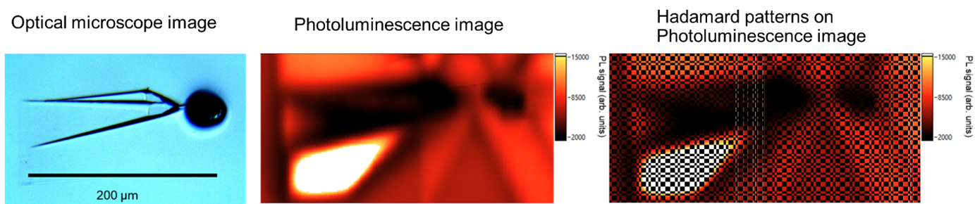
Figure 1. On the left, optical image of a polytype inclusion defect on a SiC wafer. In the middle, the spectral PL map of the same area. It is apparent that the defect affects a larger area than what can be observed in the optical image. On the right, Hadamard patterns projected on the sample during compressive sampling.
Compressed sensing has been demonstrated for spectral PL imaging measurements at NPL, through a simulation process using real measurement data. The potential for faster measurements due to undersampling has been observed, the specific noise levels to maintain a < 10 % inaccuracy were determined for the development of a CS spectral PL imaging measurement system. Ellipsometry imaging methods have been applied to SiC and GaN samples at BAM and PTB, to investigate the suitability of such techniques for wide bandgap semiconductor defect characterisation, and study the comparability of local metrology methods and the statistical significance of estimating local properties from such data. The potential for compressed sensing for the investigation of pyramid defects on GaN/SiC using imaging ellipsometry can be realised by scanning the entire sample surface and applying statistical methods. The suitability of different compressed sensing approaches for real-time data interpolation when measuring surface topography via Atomic Force Microscopy have also been investigated at CMI, with specific sampling approaches demonstrated.
20th September 2022
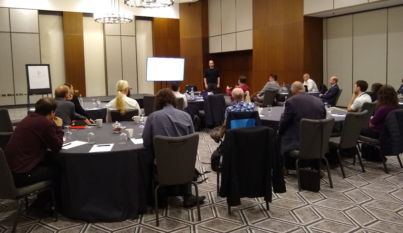
PowerElec Industry Stakeholder Workshop
Parkgate Hotel, Cardiff, 20 September 2022
CSC hosted a workshop for the PowerElec consortium along with industry stakeholders. The workshop included presentations and discussions on compound semiconductor manufacturing, metrology, device testing, and the wider innovation landscape. Content was delivered by AIXTRON, CS Connected, Compound Semiconductor Centre, IQE, KLA-SPTS, Cardiff University, Swansea University, and NPL. There we 26 attendees (5 virtual).
Presentation Topics:
- Introduction to the EMPIR PowerElec project (NPL)
- MOCVD growth of wide bandgap semiconductors for power devices (AIXTRON)
- The South Wales Compound Semiconductor Cluster (CS Connected)
- Wide bandgap epitaxial materials development (IQE)
- Wide bandgap process technology development (SPTS)
- High Frequency GaN device characterisation (Cardiff)
- Wide bandgap materials roadmap (Swansea)
- GaN capability within the South Wales cluster (CSC)
Panel Discussion (KLA, NPL, Swansea University):
Compound semiconductors are intrinsically more complex than silicon, but the applications are also very different. Silicon industry is focused on processing and memory, driven by miniaturisation, but compound semiconductors have much wider range of applications. Complexity is more about the epi-structure and material composition than lateral feature size. Metrology for CS is different from that existing for Si due to the complexity of the materials, complexity of the stacks (in some cases with hundreds of layers), larger CS bandgap which limits some measurement methods and open opportunities to use new methods.
Compound semiconductors have much more defects than Si. In Si there are typically a few defects measured per wafer, while in CS we measure a few defects per cm2. There are many defect types so it is important to identify which ones are critical in order to prioritise.
Inspection and Metrology are traditionally considered as separate disciplines, where industrial semiconductor metrology is currently limited to profilometry, scatterometry, and critical dimension. Industry relies on data-driven (AI/ML) methods for inspection, though the metrological concepts of uncertainty, calibration, and traceability are not well-defined or understood for these methods. IP considerations are a barrier to sharing information about the importance of different defect types. Companies will not disclose which defects matter most to them. The lack of documentary standards is a barrier to unambiguous discussion of defects, especially for GaN.
Automotive industry is the major pull for power electronics. They require ‘zero defects’, though it is not clear which defects matter. Innovation in power electronics is dominated by vertically-integrated companies, but over time industries are expected to specialise and outsource.
Key Messages & Conclusions:
There is massive global investment in semiconductors (bn in USA, €145bn in EU, Tn in China).
Significant growth of uptake of CS technology. CARG 2020-2026: 15%-20% in RF applications, 185% in Power applications, 100% in metaverse (mainly microdisplays).
Skills and training will be the limiting factor for growth in the UK, and elsewhere.
High throughput photoluminescence mapping is an important opportunity for defect metrology. Silicon carbide polytypes have strong photoluminescence, which could be more reliably classified with spectrally resolved measurement. Scatterometry has high sensitivity but cannot distinguish shape of particles < 10 µm.
Defect classification libraries are important for accurately describing and understanding defects. JEITA EDR-4712/100-400 provides such a library for SiC but there is no comparable document for GaN.
Metrology for controlling etching during manufacturing is important: both material defects and processing control need to be considered.
b-Ga2O3 is now receiving sustained industrial interest as a next generation material and Europe has an opportunity to lead (along with Japan).
An important challenge for process development is to determine whether defects arise from substrate quality, epi-growth, or subsequent processing. Similarly, to understand how the MOCVD tool performance changes through its lifetime. GaN reactors are cleaned between cycles, but there is no suitable process for cleaning SiC reactor.
Beyond power electronics, wide bandgap semiconductors have important applications in comms, sensing, and now especially microLED displays).